Skip to content
Skip to product content
ONTO / Nanometrics RPMBlue Photoluminescence Mapping System

ONTO / Nanometrics RPMBlue Photoluminescence Mapping System

Asset #: 157363

Make: ONTO / Nanometrics

Model: RPMBlue

Wafer Sizes: 2, 3, 4, 5, 6, 12 inch

Last Confirm Date: August 11, 2026

ONTO / Nanometrics RPMBlue Photoluminescence Mapping System, up to 6"
- Automatic Wafer Loader - Wafer Size: 2", 4" & 6" (Up to 150 mm) - Maximum Wafer Thickness: 1 mm - Industry Standard Genmark Robot & Pre-Aligner - High-Speed R-Theta Wafer Stage - Vacuum Wafer Hold-Down - Stage Rotation Speed: Up to 81 RPM - Scan Resolution: Up to 0.1 mm - Measurement Speed: Up to 2,000 Points/Second - Measurement Wavelength Range: 405–1700 nm - Excitation Sources: 405 nm, 532 nm & 980 nm - White Light Excitation Source - Spectral Measurement Option - Integrated PL Intensity Mapping - Peak Wavelength Mapping - Peak Intensity Mapping - Full-Width at Half Maximum (FWHM) Mapping - PL Wavelength Resolution: ≤0.3 nm - Peak Wavelength Reproducibility: <1 nm - White Light Thickness Measurement - Thickness Measurement Accuracy: Better Than 1% - Thickness Measurement Precision / Reproducibility: ≤1% or <10 nm - VCSEL Structure Analysis Capability - Fixed Spectrometer Entrance Slit - Automatic Recipe-Based Wafer Processing - Automatic Cassette-to-Inspection Wafer Handling - 670 nm Laser Pre-Aligner - Cleanroom Compatible

Recommended Products


Equipment Sourcing:

Unmatched Expertise in Global Procurement

See More of Our Equipment

At Bridge Tronic Global, we leverage our extensive network and industry expertise to source high-quality semiconductor manufacturing equipment from trusted suppliers worldwide. Whether you're looking for cutting-edge technology or reliable pre-owned equipment, our sourcing capabilities ensure that you receive the best options tailored to your needs.

We understand that every client's requirements are unique, so we prioritize transparency, thorough vetting, and a deep understanding of the global market to secure the right equipment for your operations. Our team is dedicated to delivering timely, cost-effective solutions without compromising on quality or performance.
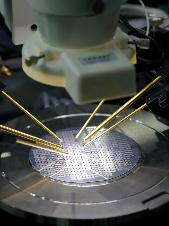

Wafer test machine

Refurbishment: Restoring Excellence, Maximizing Value

At Bridge Tronic Global, our refurbishment services breathe new life into used semiconductor manufacturing equipment, ensuring peak performance at a fraction of the cost. Our expert technicians meticulously restore equipment from leading brands like KLA and Hitachi, applying rigorous testing and quality control measures. Whether you need a single piece refurbished or a fleet of equipment overhauled, we deliver reliable, high-performing solutions that extend the lifespan of your assets while optimizing your budget.

Cart

Your cart is currently empty