Skip to content
Skip to product content
Thermo Fisher Scientific / FEI Helios NanoLab 600 FIB (Focused Ion Beam)

Thermo Fisher Scientific / FEI Helios NanoLab 600 FIB (Focused Ion Beam)

Asset #: 75427

Make: Thermo Fisher Scientific / FEI

Model: Helios NanoLab 600

Thermo Fisher Scientific / FEI Helios NanoLab 600 FIB (Focused Ion Beam)
- Dual beam
Vacuum system:
- Edwards XDS10 Scroll pump
- Sample stage: 5-Axes motorized X-Y-Z-rotate-tilt stage
- Step size: 100 nm (Minimum)
- High vacuum: 10^-10 mbar
Travel:
- X, Y-Axis: 150 mm
- Z-Axis: 10 mm
- Tilt range: -5° to +60°
Repeatability:
- 1 µm at 0°
- 2 µ at 52°
Electron optics:
- Magnetic immersion lens
- Ultrahigh brightness emitter
- Source: SCHOTTKY Field emitter
Accelerating voltage: 350 V to 30 kV (Continuously adjustable)
- Beam current: 1 pA - 22 nA
Resolution:
- 0.9 nm at 15 kV
- 1.4 nm at 1 kV
Ion optics:
- Sidewinder Field emission focused ion beam optics
- Liquid Gallium ion emitter
- Accelerating voltage: 0.5 kV to 30 kV (Continuously adjustable)
- Beam current: 1.5 pA - 20 nA
- Imaging resolution: 5 nm at 30 kV
- Milling resolution: 10 nn on Cr thin film
Scanner:
- High-resolution digital scanning engine
- Resolution: 512x442, 1024x884, 2048x1768, 4096x3536 pixels
- Minimum dwell time: 25 ns/pixel
- Electronic scan rotation by 360°
Patterning system:
- Maximum resolution: 64k x 64k
- Minimum dwell: 25 ns/pixel
- Maximum dwell: 25 ms/pixel
- Multiple pattern shapes
- Complex milling pattern through bitmap import
Detectors:
- In-lens SE and BSE True Lens Detector (TLD)
- Everhart-Thornely SE Detector (ETD)
- 14-Segments solid state STEM II detector
- Chamber viewing IR CCD camera
Controller:
- Microscope controller
- LCD Monitor, 19"
- Screen resolution: 1280x1024
- Optical mouse
- Chamber door mounted interface for manipulators
- Broad beam plasma source ion column (Focus 250 µm)
- Manuals included
- Does not include manipulator

Recommended Products


Equipment Sourcing:

Unmatched Expertise in Global Procurement

See More of Our Equipment

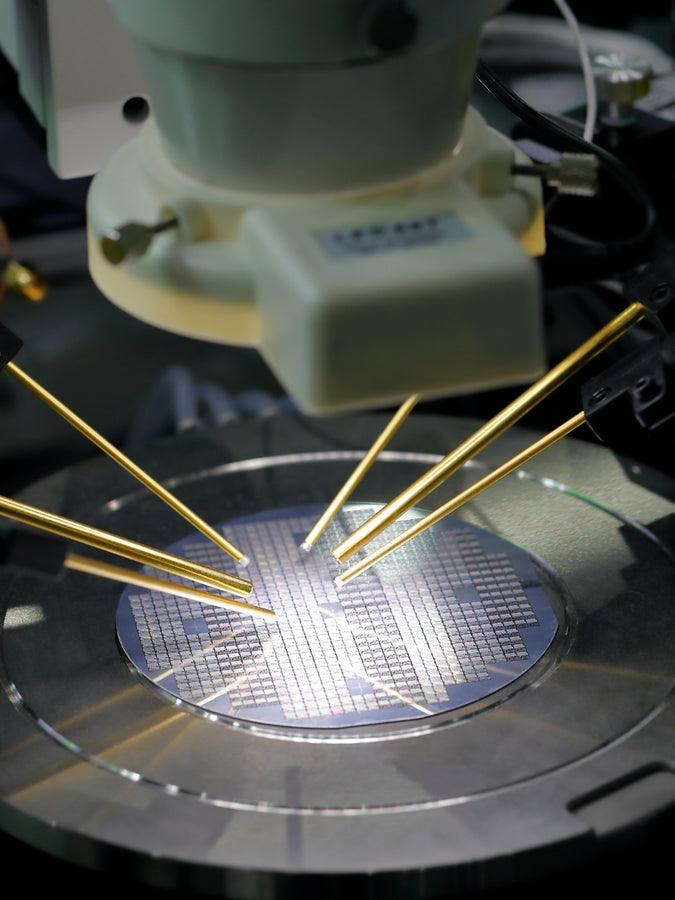
At Bridge Tronic Global, we leverage our extensive network and industry expertise to source high-quality semiconductor manufacturing equipment from trusted suppliers worldwide. Whether you're looking for cutting-edge technology or reliable pre-owned equipment, our sourcing capabilities ensure that you receive the best options tailored to your needs.

We understand that every client's requirements are unique, so we prioritize transparency, thorough vetting, and a deep understanding of the global market to secure the right equipment for your operations. Our team is dedicated to delivering timely, cost-effective solutions without compromising on quality or performance.


Wafer test machine

Refurbishment: Restoring Excellence, Maximizing Value

At Bridge Tronic Global, our refurbishment services breathe new life into used semiconductor manufacturing equipment, ensuring peak performance at a fraction of the cost. Our expert technicians meticulously restore equipment from leading brands like KLA and Hitachi, applying rigorous testing and quality control measures. Whether you need a single piece refurbished or a fleet of equipment overhauled, we deliver reliable, high-performing solutions that extend the lifespan of your assets while optimizing your budget.

Cart

Your cart is currently empty